How to Make Cell Flashlight

Want to make a flashlight by yourself? This step-by-step guide aims to outline how to design and build a fully functional single AA or AAA cell flashlight. It’s convenient to use flashlights as a light source outdoors, during power outages, in places without permanently installed lighting or when a portable light source is needed.
Below we described steps needed to understand how the solution has been programmed to create the cell flashlight. However, if you just want to get the result of programming, download GreenPAK Designer software to view the already completed GreenPAK Design File. Plug the GreenPAK Development Kit to your computer and hit the program to design the device.
How does it work?
To design a flashlight, start with building the converter using the SLG47513. The converter contains a huge amount of different macrocells which allows to easy create the circuit up to the task. The IC is a low voltage programmable mixed signal matrix that is designed to be powered from a supply in a range of 1 to 1.65 V, ideal for a single non-rechargeable battery or a NiMH cell.
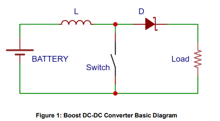
A boost converter (step-up converter) is a DC-to-DC power converter that steps up voltage (while stepping down current) from its input to the load. It is a class of switched-mode power supply (SMPS) containing at least two semiconductors (a diode and a transistor) and an energy storage element, an inductor in our case. To reduce voltage ripple, simple filters made of capacitors are normally added to such a converter’s output and input. A boost converter could be used to drive a powerful white LED, which requires a voltage of 2.7 to 3.6 V (depending on the type) from a single 1.2 or 1.5 V battery cell. Such a device is described in this guide.
Step 1 — The Design

The schematic diagram above shows the relationships between input and output voltage, current, and power are as follows:

When the switch turns ON and OFF, coil L will generate a voltage spike which is added to the Vbat boosting voltage on the load. If the output voltage rises above the desired, the switch’s turn-on period will reduce enough to maintain a stable output voltage.
Step 2— Circuit Design

The pictured flashlight circuit was designed using the SLG47513 IC and Go Configure software. It is a fully functional flashlight with two brightness modes and a single pushbutton operation.
Use the following parameters to create this design:
- Input voltage range (Vin- 0.9 to 1.65 V
- Output voltage (Vout)- 2.75 to 3.0 V
- Output current (Iout)- 25 and 100 mA PWM regulated
- PWM frequency- 400 kHz for 25 mA
- PWM frequency- 200 kHz for 100 mA
Calculated values for 25 mA:
- Min. Duty Cycle — 40%
- Max. Duty Cycle — 68%
- Min. Inductor size — 11 µH
- Peak Inductor current — 83 mA
- Filter Capacitor — 10 µF
Calculated values for 100 mA:
- Min. Duty Cycle — 40%
- Max. Duty Cycle — 67%
- Min. Inductor size — 9.9 µH
- Peak Inductor current — 333 mA
- Filter Capacitor — 100 µF
In both cases, a 10 µH 1A inductor and 100 µF low ESR capacitor will be up to the task. Also, in this circuit, a low gate threshold voltage power MOSFET must be used. Such as DMN1019UVT and BSL802SN. And it is recommended to use a lowest maximum forward voltage drop Schottky rectifier for example VS-10BQ015-M3.
Step 3— Go Configure Project

Since this boost regulator is designed to have two brightness modes (25A and 100 mA) and only one inductor, there must be two different PWM frequencies for each mode in order to ensure high efficiency. MF0 serves as a frequency divider with two outputs. CNT0/DLY0/FSM0 outputs 400 kHz for 25 mA mode and DFF14 outputs 200 kHz for 100 mA mode. The PWM logic is built on MF1 (CNT1/DLY1 and 3-L10) CNT3/DLY3, and 3-bit LUT1. The CNT3/DLY3 and CNT1/DLY1 sets the maximum duty cycle for both modes respectively. It remains at a maximum unless the feedback signal from either ACMP0H or ACMP1H through 3-L0 MUX cuts it to the width when the voltage on the current sense resistor is equal to the Vref maintaining a constant load current. The SLG47513 has relatively low current outputs which are not suitable to drive high capacitive loads (like MOSFET gate) at high frequencies. But the abundance of them allows not only to connect them in parallel increasing output current (and ability to drive MOSFET) but make a combination of push-pull and open-drain outputs. That allows controlling the switch-on and off times of the MOSFET separately. In this case, Pins 11, 12, 13, and 16 are configured as 2x push-pull outputs and are charging and discharging the gate through the R1 current limiting resistor. But Pins 3, 4, 5, 6, 8, 14, and 15 are configured as 2x open-drain outputs (1x for Pins 3 and 4) are connected to the gate directly and are only discharging its capacitance speeding up the turn-off time of the MOSFET improving the converter efficiency. The ACMPs in this design are used in a current feedback loop. The output current is determined by the ACMP’s Vref and the R2 resistance. In this case
𝑽𝒓𝒆𝒇𝟏 = 𝑰 × 𝑹 = 𝟏𝟎𝟎𝒎𝑨 × 𝟏 𝑶𝒉𝒎 = 𝟏𝟎𝟎 𝒎𝑽
or
𝑽𝒓𝒆𝒇𝟐 = 𝑰 × 𝑹 = 𝟐𝟓𝒎𝑨 × 𝟏 𝑶𝒉𝒎 = 𝟐𝟓 𝒎𝑽
Setting 25 mV referense for ACMP0H and 100mV for ACMP1H. The combination of macrocells MF2, MF4, and CNT5/DLY5 make up the logic that allows the user to operate the flashlight using only one push button. A long press (> 1 s) will turn on/off the device, and a short press (< 1 s) will switch between the two modes. Pin 9 is configured as a digital input with a Schmitt trigger and a 10k pull-up resistor. This setting ensures very stable work without any external components. The CNT4/DLY4 is set as a 32 ms delay filtering out any button noise eliminating the need for an external capacitor. DFF18 latches one of two selected modes. Its output goes to two MUXs: 3-L10 which selects the PWM frequency and 3-L0 selects between ACMPs with different Vrefs. The CNT2/DLY2 is set to 1 s delay and together with DFF14 enables or disables both ACMPs and OSC1. So, when the device is OFF, all digital macrocells are static and analog ones are disabled except OSC0. In this state, current consumption is less than 2 µA. The CNT5/DLY5 ensures the device will not switch modes while powering on/off.
Step 4— Printed Circuit Board to Test the Design
For testing purposes, a PCB was designed.

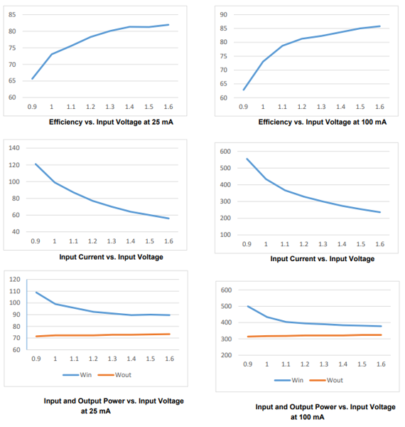
Step 5— Device Testing Results

Conclusion
As can be seen, designing and building a fully functional flashlight powered by a single AA or AAA battery cell is relatively easy using the SLG47513 IC. As an alternative, the SLG47512 IC could be used instead. The only difference is fewer output pins resulting in lower output current but still, it should be enough to drive the MOSFET. Both chips have all required macrocells and the circuit uses minimum external components which makes it very cost-effective. Should be noted that highly flexible Vref settings along with the current sense resistor allow setting almost any output current required by the LED.
